-

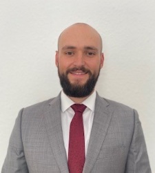
David Mawby
Director and Co-Founder
KuasaSemi Ltd
主題
TCAD tools for wide bandgap Power device development講師簡介
Education: Bachelor’s Degree Electrical and Electronic Engineering, Cardiff University, UK.
Experience:David is director and co-founder of KuasaSemi Ltd. He is an experienced software and electronics engineer. He has previously worked as the lead electronics engineer at a leading UK renewable energy company. He also has experience in the semiconductor industry working on integrated circuit applications. He has been working on the TCAD software for WBG Power devices at KuasaSemi for over 1 year now.
演講大綱
There are multiple modelling difficulties that make the design of wide bandgap devices using traditional TCAD software more challenging than equivalent silicon technologies.
These challenges arise from the fundamental WBG physical material properties. In terms of process modelling WBG materials such as SiC and GaN do not have appreciable diffusion of implanted impurities. This makes the modelling of implanted profiles critical in optimizing device performance. Crystal orientation clearly has a significant effect if channeling effects come into play. Gate oxidation dynamics are significantly slower in SiC than in Silicon. GaN devices are defined by the epitaxial process used to define the structures. However, in terms of process modelling this can be defined using simple geometric descriptions.
The physics of the devices being modelled models need to have a careful description of the defects. However, one of the most difficult aspects of wide bandgap modelling appears during reverse bias – especially breakdown characteristics, this arises from the very small intrinsic carrier concentration resulting in a much bigger number range than for silicon. As mentioned above, the bulk and interface defects need special attention when modelling WBG devices, we will discuss this in the presentation, and explain how this is implemented in our new simulation code.