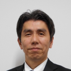
-

倉又 朗人
CEO
Novel Crystal Technology, Inc
主題
Ga2O3 Single Crystal Wafers for Power Device Applications講師簡介
Education:He received the B.E degrees from Kyoto University, Kyoto, Japan, in 1986.
Experience:He joined Fujitsu Laboratories Ltd., Atsugi, Japan, in 1986 and became a manager in 1999. He moved to Eudyna Devices Inc., Yokohama, Japan, in 2005, as a manager. He moved to Tamura Corporation, Sayama, Japan, in 2008 as a senior manager. He established Novel Crystal Technology, Inc. in 2015 and became a CEO. He has been engaged in research and development of crystal growth and device process for compound semiconductor devices such as laser diodes, optical detectors, diodes, transistors and so on.
演講大綱
Ga2O3 is expected to be used as a material for next generation power devices. When considering material selection for power devices, the availability of native substrates is important. Ga2O3 meets this requirement. This presentation will report on wafer fabrication technology of Ga2O3. We report two bulk crystal growth techniques. One is the EFG method, and another is the vertical Bridgman (VB) method. We also report on epitaxial growth technology using the HVPE method.